- 您现在的位置:买卖IC网 > Sheet目录323 > DSP56311EVM (Freescale Semiconductor)KIT EVALUATION FOR DSP56311
�� �
�
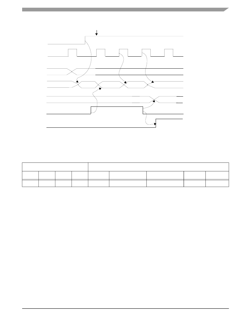
�Operating� Modes�
�Mode� 4� (internal� clock):� TRM� =� 1� first� event�
�N� =� write� preload�
�M� =� write� compare�
�TE�
�Clock�
�(CLK/2� or� prescale� CLK)�
�TLR�
�N�
�Counter�
�0�
�N�
�N+1�
�M�
�N+� 1�
�Next� 0-to-1� edge�
�TCR�
�TIO� pin�
�TCF� (Compare� Interrupt� if� TCIE� =� 1)�
�width� being� measured�
�M�
�on� TIO� starts�
�counter� from� current�
�count� and� process�
�repeats.� Overflow�
�may� occur� (TOF� =� 1).�
�Interrupt Servic� e�
�reads� TCR� for�
�accumulated� width�
�NOTE:� If� INV� =� 1,� a� 1-to-0� edge� on� TIO� loads� the� counter,� and� a� 0-to-1� edge� on� TIO�
�of� M� -� N� clock� periods.�
�stops� the� counter� and� loads� TCR� with� the� count.�
�Figure� 9-12.� Pulse� Width� Measurement� Mode,� TRM� =� 0�
�9.3.2.2� Measurement� Input� Period� (Mode� 5)�
�Bit� Settings�
�Mode� Characteristics�
�TC3�
�0�
�TC2�
�1�
�TC1�
�0�
�TC0�
�1�
�Mode�
�5�
�Name�
�Input� period�
�Function�
�Measurement�
�TIO�
�Input�
�Clock�
�Internal�
�In� Mode� 5,� the� timer� counts� the� period� between� the� reception� of� signal� edges� of� the� same� polarity�
�across� the� TIO� signal.� The� value� of� the� INV� bit� determines� whether� the� period� is� measured�
�between� consecutive� low-to-high� (0� to� 1)� transitions� of� TIO� or� between� consecutive� high-to-low�
�(1� to� 0)� transitions� of� TIO� .� If� INV� is� set,� high-to-low� signal� transitions� are� selected.� If� INV� is�
�cleared,� low-to-high� signal� transitions� are� selected.� After� the� first� appropriate� transition� occurs� on�
�the� TIO� input� signal,� the� counter� is� loaded� with� the� TLR� value.� On� the� next� signal� transition� of� the�
�same� polarity� that� occurs� on� TIO� ,� TCSR[TCF]� is� set,� and� a� compare� interrupt� is� generated� if� the�
�TCSR[TCIE]� bit� is� set.� The� contents� of� the� counter� load� into� the� TCR.� The� TCR� then� contains� the�
�value� of� the� time� that� elapsed� between� the� two� signal� transitions� on� the� TIO� signal.� After� the�
�second� signal� transition,� if� the� TCSR[TRM]� bit� is� set,� the� TCSR[TE]� bit� is� set� to� clear� the� counter�
�and� enable� the� timer.� The� counter� is� repeatedly� loaded� and� incremented� until� the� timer� is�
�disabled.� If� the� TCSR[TRM]� bit� is� cleared,� the� counter� continues� to� increment� until� it� overflows.�
�DSP56311� User’s� Manual,� Rev.� 2�
�Freescale� Semiconductor�
�9-13�
�发布紧急采购,3分钟左右您将得到回复。
相关PDF资料
DSPAUDIOEVMMB1E
BOARD MOTHER DSP563XX
DSPIC30F2010 DEVELOPMENT KIT
KIT DEV EMBEDDED C
DSTRM-KT-0181A
DSTREAM DEBUG AND TRACE UNIT
DSUT1CSU
SURGE SUPPR NETWORK W/GROUND
DTEL2
SURGE SUPPRESSOR PHONE RJ11/RJ45
DV003001
PROGRAMMER PICSTART PLUS 16C/17C
DV164035
MPLAB ICD3 IN-CIRC DEBUGGER
DV164039
KIT DEV PIC24FJ256DA210
相关代理商/技术参数
DSP56311EVMIG_D
制造商:未知厂家 制造商全称:未知厂家 功能描述:DSP56311EVMIG DSP56311EVM Sample Code
DSP56311EVMUM
制造商:未知厂家 制造商全称:未知厂家 功能描述:DSP56311 Evaluation Module Hardware Reference Manual
DSP56311FACT
制造商:未知厂家 制造商全称:未知厂家 功能描述:DSP56311 Higher performance programmable DSP for demanding voice and data applications
DSP56311UM
制造商:未知厂家 制造商全称:未知厂家 功能描述:DSP56311 24-Bit Digital Signal Processor Users Manual
DSP56311UMAD
制造商:未知厂家 制造商全称:未知厂家 功能描述:DSP56311 Users Manual Addendum
DSP56311VF150
功能描述:数字信号处理器和控制器 - DSP, DSC 150Mhz/300MMACS 150Mhz EFCOP RoHS:否 制造商:Microchip Technology 核心:dsPIC 数据总线宽度:16 bit 程序存储器大小:16 KB 数据 RAM 大小:2 KB 最大时钟频率:40 MHz 可编程输入/输出端数量:35 定时器数量:3 设备每秒兆指令数:50 MIPs 工作电源电压:3.3 V 最大工作温度:+ 85 C 封装 / 箱体:TQFP-44 安装风格:SMD/SMT
DSP56311VF150B1
功能描述:数字信号处理器和控制器 - DSP, DSC 24 BIT DSP
RoHS:否 制造商:Microchip Technology 核心:dsPIC 数据总线宽度:16 bit 程序存储器大小:16 KB 数据 RAM 大小:2 KB 最大时钟频率:40 MHz 可编程输入/输出端数量:35 定时器数量:3 设备每秒兆指令数:50 MIPs 工作电源电压:3.3 V 最大工作温度:+ 85 C 封装 / 箱体:TQFP-44 安装风格:SMD/SMT
DSP56311VF150R2
功能描述:数字信号处理器和控制器 - DSP, DSC 24 BIT DSP RoHS:否 制造商:Microchip Technology 核心:dsPIC 数据总线宽度:16 bit 程序存储器大小:16 KB 数据 RAM 大小:2 KB 最大时钟频率:40 MHz 可编程输入/输出端数量:35 定时器数量:3 设备每秒兆指令数:50 MIPs 工作电源电压:3.3 V 最大工作温度:+ 85 C 封装 / 箱体:TQFP-44 安装风格:SMD/SMT